
A PCB-fabrication + PCBA-process risk screening of the ACube "PORTATILE" · NXP T2080 10-layer motherboard, built from its own drill / netlist / artwork / BOM data and checked against the IPC/J-STD family. This is not a manufacturing release review.
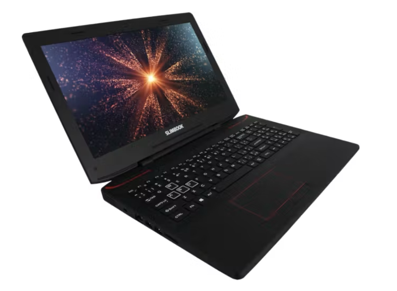
Baseline reviewed: the released design at revision ACB_0001_2 (NC-drill dated 2022-08-08). Board ≈ 289.6 × 148.7 mm, 10 copper layers, through-vias only, double-sided SMT (2,047 placements). Every figure below comes directly from the board's own released design data.
A single verdict is not used. Each decision is dispositioned against its blocking findings.
| Decision | Disposition |
|---|---|
| Engineering prototype (design) | CONDITIONAL |
| PCB quotation-ready | NO |
| PCB fabrication-ready | NO |
| PCBA prototype process | CONDITIONAL |
| Pilot production | NO |
| Volume production | NO |
Minimum pre-build blockers: release the fab-documentation package; select & approve the surface finish (not by default); fab sign-off of the 8:1 aspect ratio and BGA via-in-pad; release the panel drawing; complete fabricator DFM and CM stencil/MSL review; close ICT/test access.
S / O / D on a 1–10 scale; Action Priority is severity-first. Each finding names the governing standard; unknowns are treated as open risk, not neutral.
| ID | Finding | S | O | D | AP | Standard | Recommended action |
|---|---|---|---|---|---|---|---|
| DFM-01 | No released fab-doc package (fab drawing, ordered stack-up, impedance table, IPC class, thickness tol). CAD holds material/impedance engineering only. | 9 | 7 | 8 | High | IPC-6012 · A-600 | Produce fab package; export stack-up + impedance table; fab sign-off |
| DFM-02 | Through-via-only, 0.20 mm min drill on 1.6 mm = 8.0:1 (drill) ≈10.7:1 (finished) worst-case aspect ratio; 4,533 such vias (95% of holes). | 7 | 6 | 6 | High | IPC-6012 | Fab sign-off of aspect ratio & hole-wall reliability |
| DFM-03 | T2080 896-ball BGA (0.8 mm, 25×25 mm) escaped with through vias; via-in-pad treatment not in data — confirmation required. | 8 | 5 | 7 | High | IPC-7095 · 4761 | Confirm via-in-pad fill/planarize; X-ray criteria |
| DFM-05 | PCB surface finish not specified for 896-ball BGA + 0201. Do not default to ENIG — select by trade study. | 8 | 6 | 5 | High | IPC-6012 · A-610 | Surface-finish trade study; fab + CM approval |
| DFM-06 | No real panel/depanel drawing (drawing rasters are donor-board photos, OCR-verified). 290×149 board with cut-outs. | 6 | 6 | 5 | High | IPC-A-600 | Panel drawing: fiducials/coupons/tabs, support under cut-outs |
| DFM-08 | Material grade generic FR-4; Dk conflict (3.7 vs 4.4–4.7 vs 4.8); no Tg/Td/CAF for lead-free reflow. | 5 | 5 | 5 | Medium | IPC-6012 | State laminate + Tg/Td/CAF; resolve Dk with fab |
| PROC-04 | 0201 (159×) + large pads + potential via-in-pad on one stencil. Step-stencil not yet justified by aperture calculation. | 6 | 6 | 5 | Medium | IPC-7525 | Compute area ratios (≥0.66); size step-stencil only if proven |
| PROC-06 | MSL handling undefined (no BOM MSL column). BGA/LGA/QFN need bake-and-bag or popcorn/delam. | 8 | 5 | 6 | High | JEDEC J-STD-020 · J-STD-033 | Per-part MSL list; floor-life/bake per J-STD-033 |
| PROC-09 | Footprint library not standardized: 113 package strings incl. duplicates; not verified vs land patterns. | 4 | 5 | 6 | Medium | IPC-7351 | Footprint validation vs mfr land patterns; dedupe |
| DFM-10 | ICT/test access: 1,482/1,691 nets accessible, 209 no-access, 108 TPs (6.4%); probe side not encoded → bottom-side ICT coverage unknown; tented-via status unconfirmed. | 7 | 6 | 7 | High | IPC-9252 / D-356 | Bottom-side probe-access study; probe rules; boundary-scan (J3 JTAG); test before thermal/chassis |
ICT probes bottom-side pads and vias against the netlist, so testability is a design property to check now, not after build. From the board's ODB++ CAD netlist (the IPC-D-356 equivalent):
Because the netlist does not encode probe side, the true bottom-side single-side ICT node coverage cannot be derived from the data — it must be produced by a DFT/fixture tool against the soldermask and pad geometry (IPC-9252 / IPC-D-356). Required actions: quantify structural fault coverage; enforce probe rules (pad Ø ≥ 0.9 mm, ≥ 50-mil grid pitch, single-side bottom access, no tented vias on probed nets); add boundary-scan (JTAG/COP, header J3) for the T2080 BGA nets ICT cannot reach; and provide current-limited power-up and shorted-rail isolation — all before the expensive thermal/chassis integration. A tented-via or bottom-access shortfall found here is a layout fix, so it is cheapest to close pre-fabrication. (Finding DFM-10.)
The DFM readiness scorecard averages ≈ 3.7 / 5 across 14 categories, with 9 categories at High (≥4) and surface finish scored 5 (unknown critical characteristic). Per the override rules, an unknown critical characteristic and open pre-build High items block release regardless of the average. The full 23-sheet workbook holds the rubric, per-category evidence and formulas.
Download the evidence workbook (XLSX) →
Reviewed design: the open-hardware GNU/Linux PowerPC Notebook by Roberto Innocenti & the Power Progress Community — powerpc-notebook.org · design files (GitLab). Product Engineer LLC is independent and not affiliated with the project.
Every figure and finding on this page comes directly from the board's own released design data — the Excellon NC-drill tool tables, the ODB++ CAD netlist, the Gerber artwork (copper + solder-paste layers), the released BOM and the native board record. Every figure is reproducible by re-running the same extraction against the released design package, and each conclusion is checked against the manufacturing standards below.
Design data © the Power Progress Community (open hardware). Detailed source-data provenance and per-finding citations are recorded in the accompanying evidence workbook.