An independent manufacturability risk screening of an open-hardware notebook motherboard. Every finding is read from the design's own files and measured against industry manufacturing standards — ending in a clear, decision-by-decision verdict.
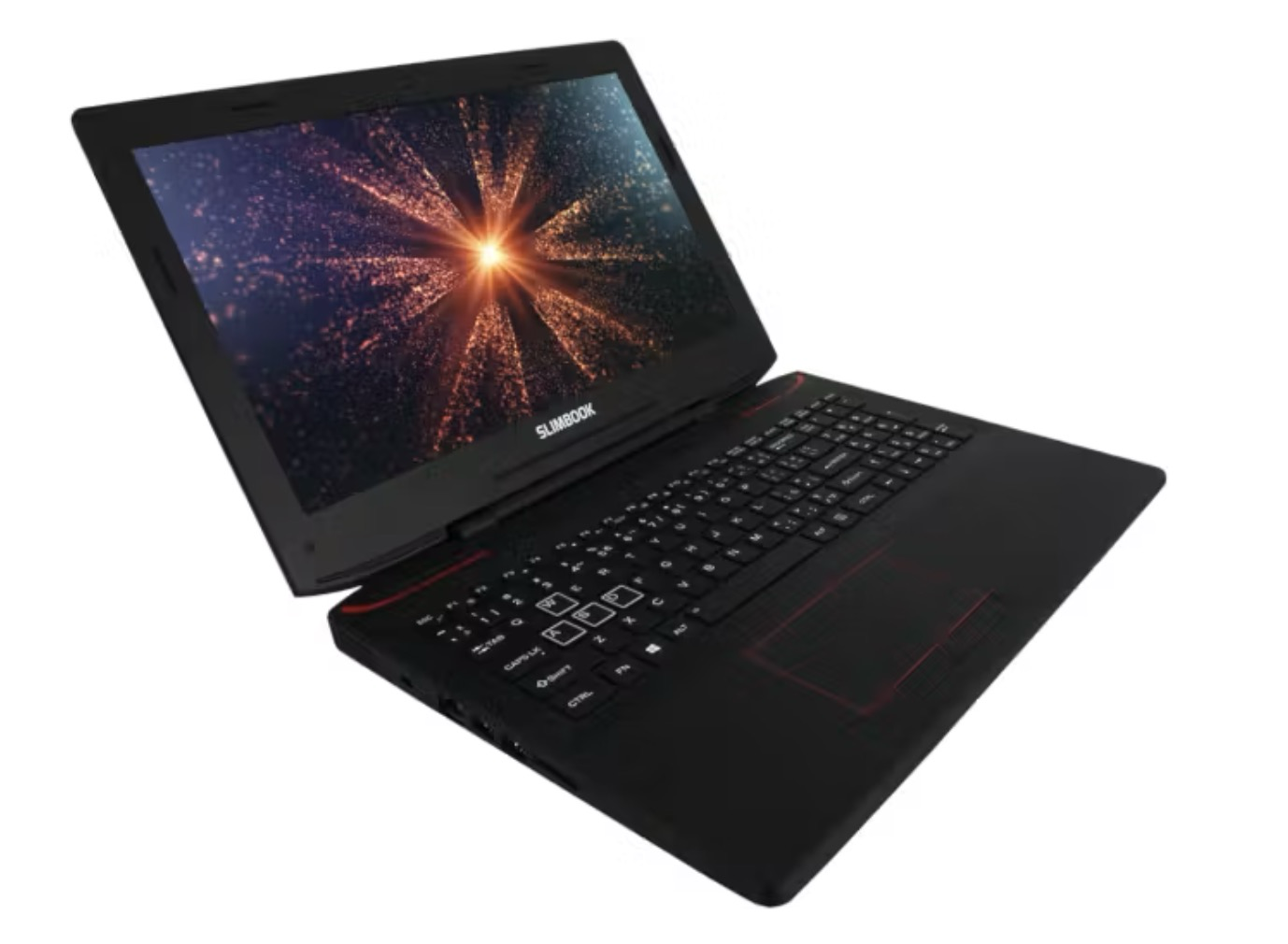
The motherboard reviewed here belongs to the GNU/Linux Open Hardware PowerPC Notebook — a rare thing in modern computing: a laptop whose electronics are designed in the open, by a community, for anyone to study, build and improve. Founded by Roberto Innocenti and developed by the Power Progress Community, the project has released the complete schematics, board layout and CAD files of a notebook motherboard built around the NXP T2080 processor. It is a serious, multi-year engineering effort toward open, user-controlled computing — and exactly the kind of design that deserves a careful manufacturability review before real money is spent building it.
Original design & files © the Power Progress Community, published as open hardware. Reviewed here independently.
One question drives this review: how ready is this motherboard to be manufactured — and at what stage? Rather than judge the design from a distance, the review works directly from the design's own released files — the actual drill tables, copper artwork, connection lists and parts list. Every number on this page was read out of those files; where the data doesn't answer a question, the gap is named rather than assumed away.
Reference: all figures parsed from the project's openly released design package — drill tables, layer artwork, netlist and bill of materials (gitlab.com/power-progress-community/oshw-powerpc-notebook).
The review starts with the raw design files and builds the engineering picture step by step — each step feeding the next — ending in the manufacturability and assembly screening.
Reference: the project's open-hardware design package — schematics, layer artwork, drill files, CAD databases and bill of materials, as released by the Power Progress Community.
Before judging how buildable the board is, the review rebuilds a picture of what it actually is. At the heart sits the NXP T2080 processor, soldered permanently to the board. Around it, the design deliberately keeps the parts people most often upgrade or replace — the memory, the graphics card and the storage — on plug-in modules, while the display connection, the ports and the power path are wired in. That one map explains a great deal: the manufacturing difficulty concentrates in a small, dense area around the soldered processor and its wiring, while the plug-in modules keep the rest of the machine serviceable and upgradeable. It is also the map that tells the screening where to look hardest — which is exactly where the verdicts below come from.
Reference: connectivity reconstructed from the project's released schematics; module and connector choices confirmed against the board CAD databases and the system parts list.
One overall verdict would hide more than it reveals. Each manufacturing decision gets its own answer, based only on the findings that block that specific decision.
| Decision | Disposition |
|---|---|
| Engineering prototype — build a few boards to learn from | CONDITIONAL |
| Send the board out for fabrication quotes | NO |
| Release the bare board for fabrication | NO |
| Assemble the prototype boards | CONDITIONAL |
| Pilot production | NO |
| Volume production | NO |
Reference: dispositions carried from the DFM and DFA screening reports; acceptance criteria aligned to published IPC/JEDEC fabrication, assembly and test standards (IPC-2221, IPC-6012, IPC-A-610, J-STD-001, IPC-9252).
Two narrative screening reports and one 22-sheet evidence workbook carrying every finding, calculation, scorecard and open action.
The motherboard is a credible, well-organized open-hardware design. It is a sound candidate for an engineering prototype once a defined list of pre-build items is closed — completing the factory documentation package, choosing the board's surface finish, obtaining the board maker's written confirmation on the few features that push normal manufacturing limits, and closing the in-circuit test (ICT) access plan while it is still a cheap layout fix. It is not yet approved for fabrication release, pilot or volume production: those decisions need released factory data, written supplier confirmation and measured results from a pilot build — none of which exist yet.
Notably, the community's own path mirrors this screening's findings: having built prototypes and worked through hardware bring-up, they have pivoted to validating the compute platform as a desktop board first — a disciplined de-risking step that clears the very gates identified here, with the notebook to follow on a proven core.
Reference: assessed against published IPC and JEDEC standards, including IPC-2221, IPC-2226, IPC-6012 (fabrication), IPC-7095 (BGA), IPC-4761 (via protection), IPC-7351, IPC-7093, IPC-7525, IPC-A-600, IPC-A-610, J-STD-001, IPC-9252/D-356 (test access) and JEDEC J-STD-020/033 (moisture sensitivity). Every finding in the reports names its governing standard; full citations are carried in the evidence workbook.
This review would not exist without the open-hardware design it studies. The motherboard is part of the GNU/Linux Open Hardware PowerPC Notebook — "an Open Hardware project for everyone, a PowerPC Notebook & Desktop for you" — founded by Roberto Innocenti and developed by the Power Progress Community, who released the complete schematics, PCB layout and CAD as open hardware.
All design files reviewed here are the community's own, published openly. We warmly appreciate the outstanding work of Roberto Innocenti and every contributor keeping open, user-controlled computing hardware alive. Since this design was published, the community has taken the classic route of seasoned hardware teams: prove the compute platform in the simplest enclosure first — a desktop variant — then bring the battery-powered notebook to life on that validated core. It is exactly the discipline this kind of design deserves. Learn about the project at powerpc-notebook.org and explore the design files at gitlab.com/power-progress-community/oshw-powerpc-notebook.
Product Engineer LLC is not affiliated with the Power Progress Community; this manufacturability screening is an independent analysis based on their openly published design.